Ddr2 Ram Circuit Diagram
Calculating ram memory capacity from schematic symbol Ram memory structure access random basic write powerpoint read ppt presentation chip logic data lines address select Ram read/writer
RAM Read/Writer
Ram symbol schematic memory capacity calculating bus address bit width there if I just realised ddr4 ram has a bulge at the coonnectors. why is that Am571x support for dual die ddr3
Ddr3 memory pcb altium cpu route example routing fan figure directives blankets create used groups class designer
Ddr3 ddr4 ddr2 ddr1 physically difference notch ddr5 mrdustbinProject ram.bo32 Schaltplan schemaHow to route ddr3 memory and cpu fan-out.
Ram memory circuit cell binary circuits watson bit figure latech eduDdr4 ram schematic has spec anandtech realised bulge just good why jedec reading features short some Ram memory cell binary watson write read circuits input access random bc line output latech eduHow to identify ddr1 ddr2 and ddr3 ddr4 ram physically.

Ram read schematic writer circuit circuits seventransistorlabs electronic
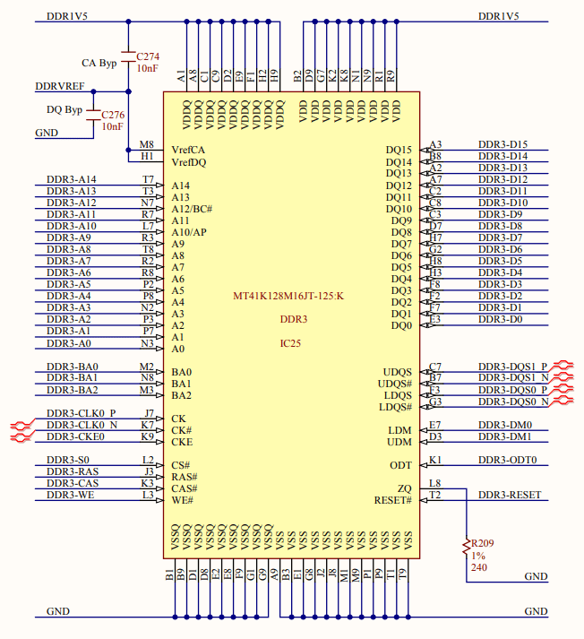
Ddr3 datasheet ddr e2e advise processors .
.


I just realised ddr4 ram has a bulge at the coonnectors. Why is that

How to Route DDR3 Memory and CPU Fan-Out | PCB Design Blog | Altium

How to identify ddr1 ddr2 and ddr3 ddr4 ram physically - mrDustBin

Project RAM.Bo32 | hc12web.de
Calculating RAM memory capacity from schematic symbol - Electrical

RAM Read/Writer

Watson

Watson